


Today’s article offers a comprehensive review of the GeForce RTX 5080 and builds on the launch article for the RTX 5090, which I will of course also link to below. But I’ll save myself redundant content and concentrate more on the card. Various performance values have already been reported and leaked and it will certainly be more interesting to focus on the accompanying circumstances today. Is the new GeForce RTX now more efficient than the RTX 4080 (Super) and, above all, who gets any added value from buying such a card? Because as the headline makes clear: Owners of Ada cards from a GeForce RTX 4070 Ti Super upwards will probably only get a sidegrade. But let’s wait for the test….

The NVIDIA GeForce RTX 4080 Super was launched in January 2024 at a recommended retail price (RRP) of 999 US dollars. The GeForce RTX 5080, which will be launched on January 30, 2025, will also be offered at an RRP of 999 US dollars. Of course, you have to factor in the usual surcharge due to VAT and greedy retailers. I’ll spoil it in advance by saying that the rumored performance increases are true, which also puts the price into perspective.
The GeForce RTX 5090 presented last week is NVIDIA’s new flagship and once again a typical Halo product aimed exclusively at well-heeled enthusiasts and prestige-oriented high-end users. It represents what is technically possible by offering maximum performance and the latest features of the new generation and is aimed at those who have the financial means to pay the premium price for this exclusivity. With its capabilities, the RTX 5090 serves a niche in which budget considerations play no role. For this target group, the card is not only a tool, but also a pure prestige object that reflects the best of technology.
The GeForce RTX 5080, on the other hand, appeals to a broader but still demanding customer base. As a top-of-the-range model, it offers a slightly more humane price/performance ratio, even if it still represents a considerable investment. It is intended for users who are willing and able to pay for high performance and future-proofing without having to pay the top prices of a Halo product. With its enormous computing power, which is usually easily sufficient for gaming in 4K resolution at maximum settings, advanced ray tracing and demanding creative applications, the RTX 5080 hits the nerve of those buyers who demand performance at the highest level, but do not completely lose sight of common sense in the cost-benefit analysis and still have their lives under control. It is therefore an ideal model for anyone who values quality and innovation without going to the absolute top of the price scale.
It was, as always, a tour de force and I have also completely adapted the game selection and expanded it to a total of 11 games, each in five different settings. There is also a brand new test system and updated metrics. The GeForce RTX 5080, which will follow shortly, will then be added in the same way. I would also like to point out in advance that I have not disassembled the GeForce RTX 5090 FE as usual this time and the teardown is (still) missing. This is because I still need the card in its original state for further tests and the process of teardown and subsequent reconstruction is so complex that it cannot be guaranteed that the card will be able to operate in the same state afterwards (liquid metal that can only be removed mechanically).
Another follow-up to the review will focus on workstation performance and professional applications. This part has been split off as a separate article, because due to driver problems and other technical details that needed to be clarified, some tests were postponed by me in order to ensure a fair and comprehensive evaluation. After all, if there is a changed driver after all, I won’t save myself the trouble of retesting, but I will save myself the superfluous export of extensive chart graphics. And so I can pack in today’s GeForce RTX 5080 at the same time and save on redundant content.
But that shouldn’t stop me from comparing the new card today with the GeForce RTX 4080 Super in particular and the entire Ada lineup of suitable Super cards in general. I’m also leaving out Ampere this time due to time constraints, but since there are enough comparisons between Ada and Ampere on my site, this is certainly easy to get over.
The GB203-400-A1 GPU in detail
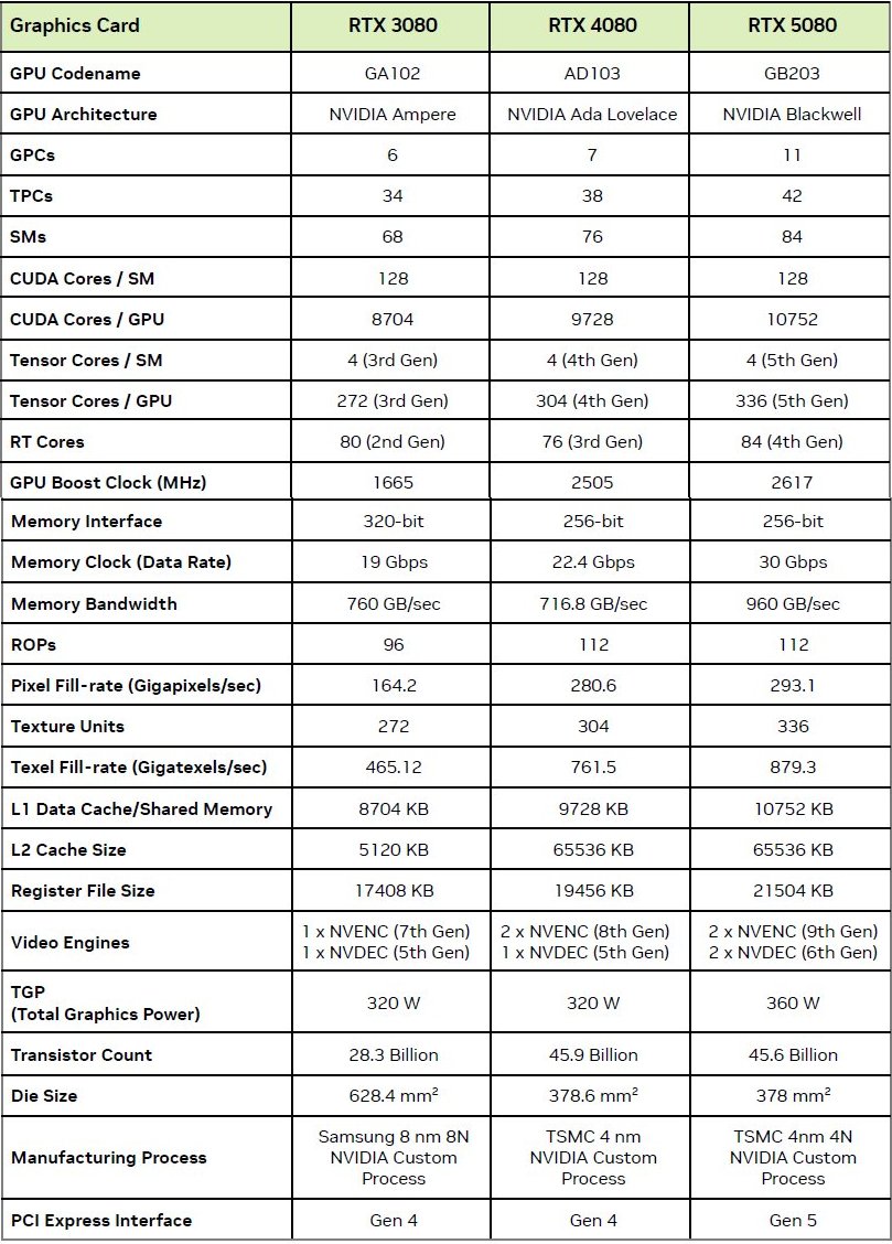
The NVIDIA GeForce RTX 5080 is based on the new Blackwell architecture and offers improvements over previous generations. The GB203-400-A1 GPU is manufactured using 4 nm production technology and comprises 45.6 billion transistors on a chip area of 378 mm². With 10,752 CUDA cores, a base clock of 2.30 GHz and a boost clock of 2.62 GHz, the card offers high computing power for current applications. It is equipped with 16 GB GDDR7 memory, which operates at 30 Gbps and achieves a memory bandwidth of 960 GB/s via a 256-bit interface.
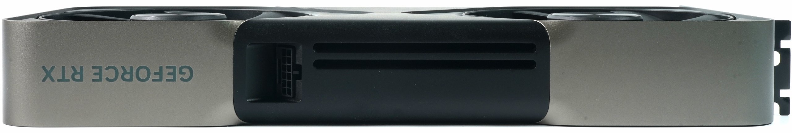
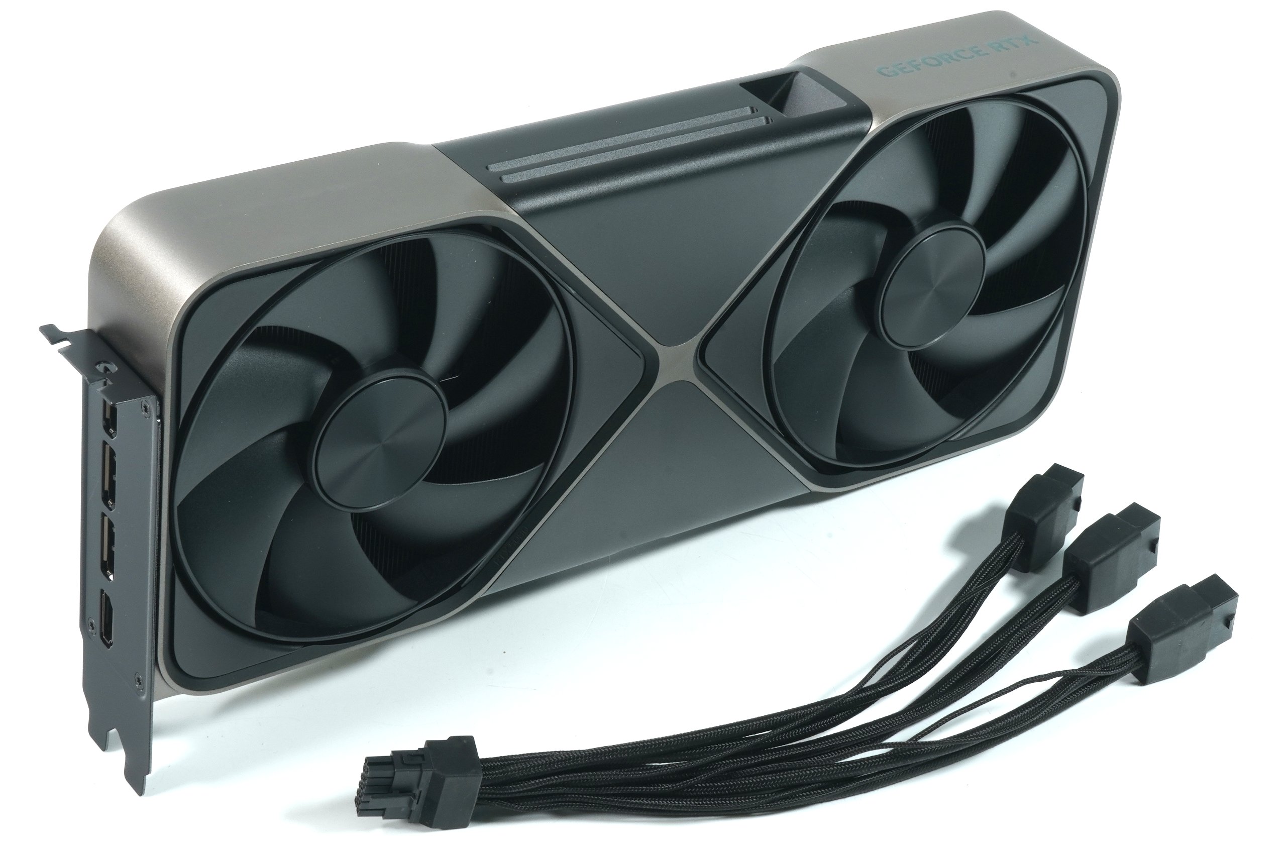
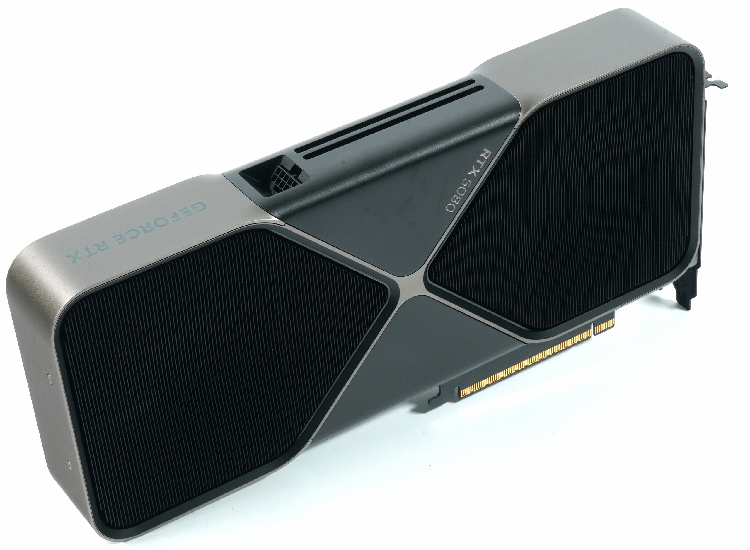
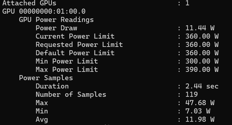
The GeForce RTX 5080 has 84 fourth-generation ray tracing cores and 336 fifth-generation tensor cores, which significantly improve performance in the area of AI-supported calculations and real-time ray tracing. The L2 cache has been increased to 64 MB to minimize data transfer bottlenecks. With a Thermal Design Power (TDP) of 360 watts, a power supply unit with at least 850 watts is recommended, whereby the connection is made via the familiar 2V2X6 power connector.

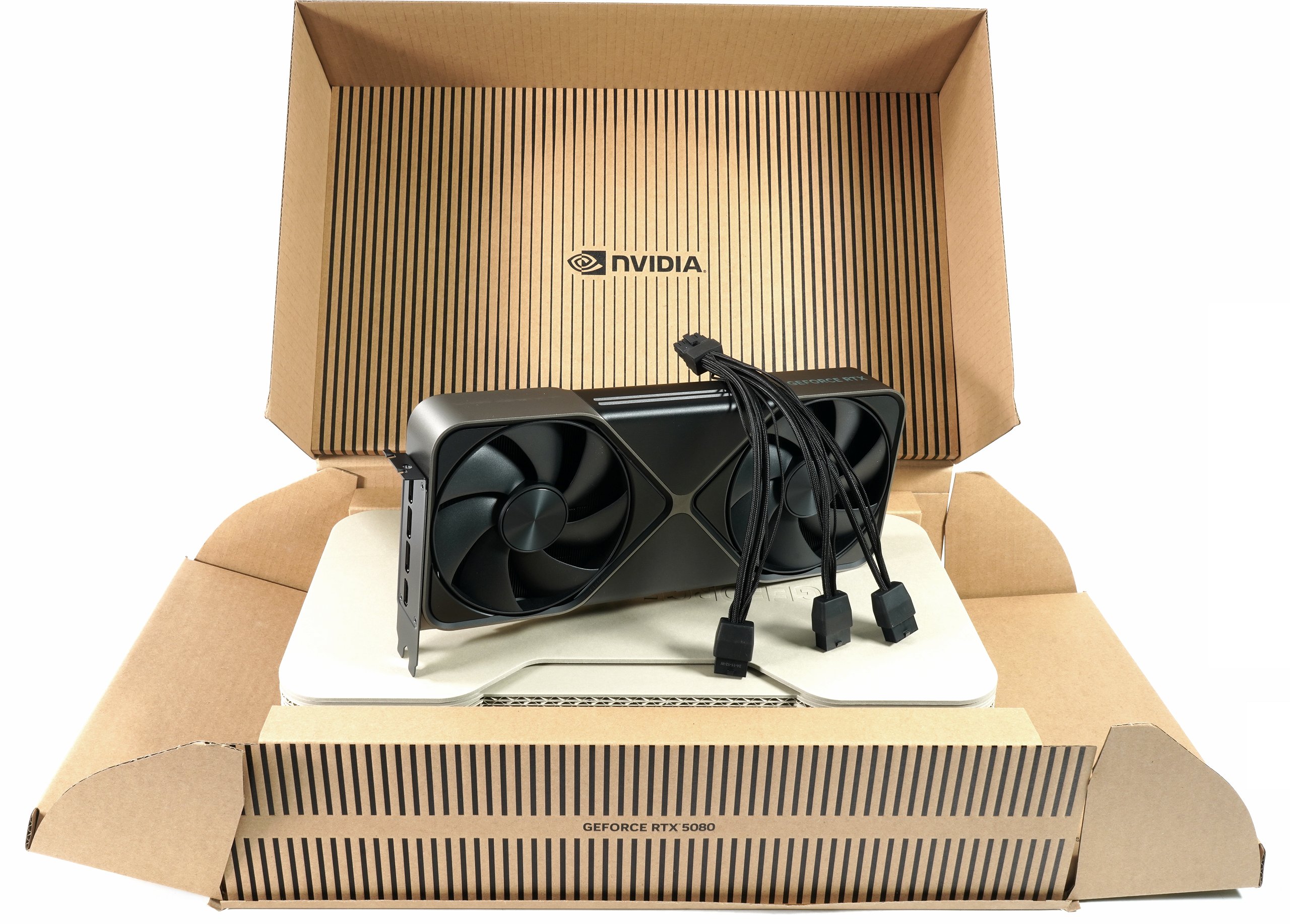
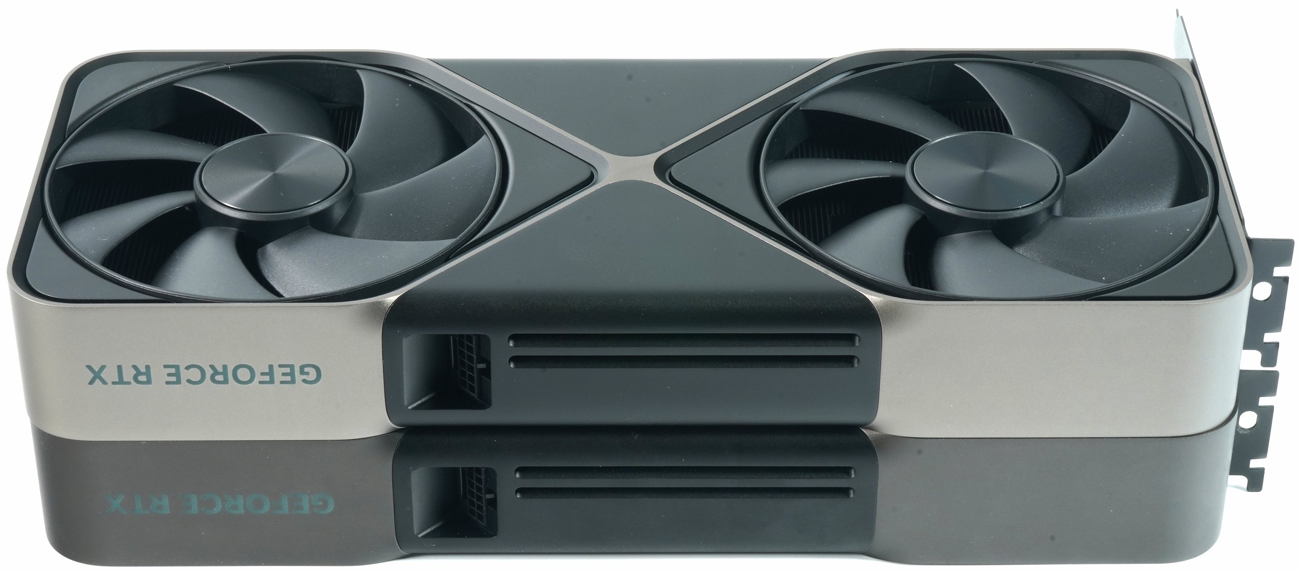
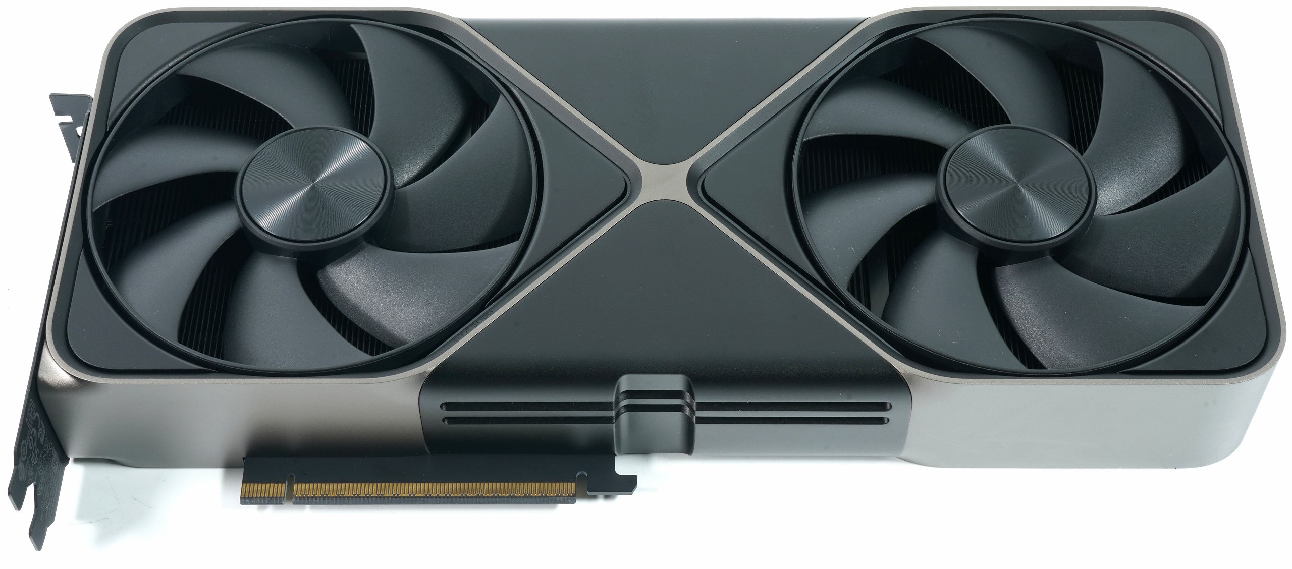
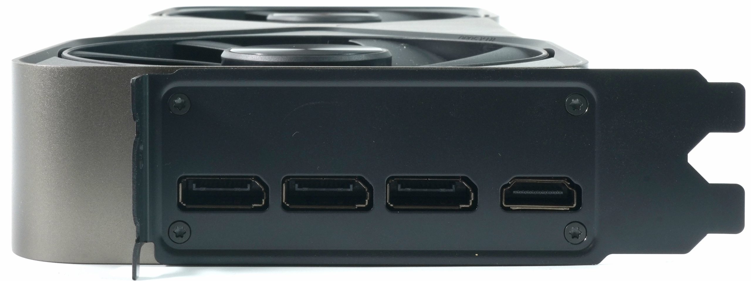
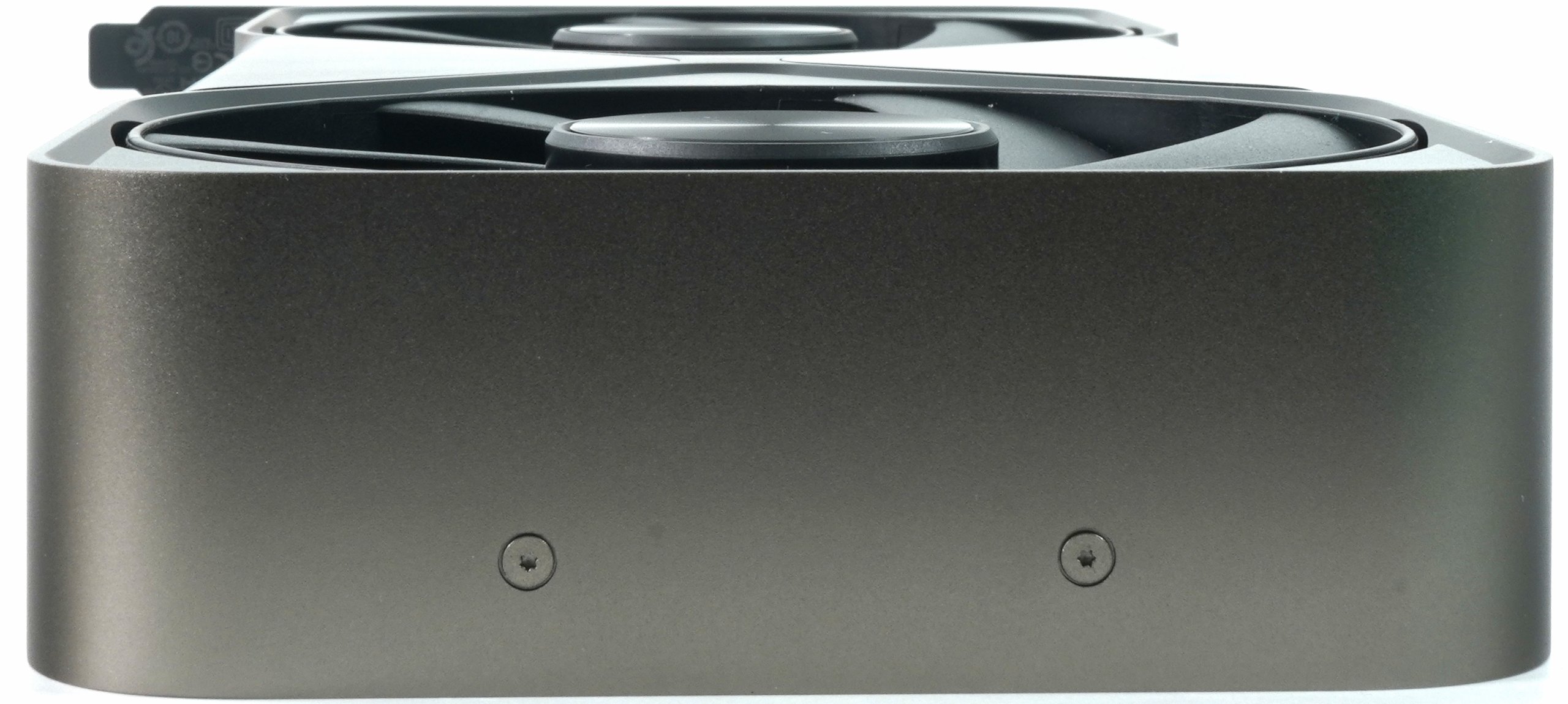
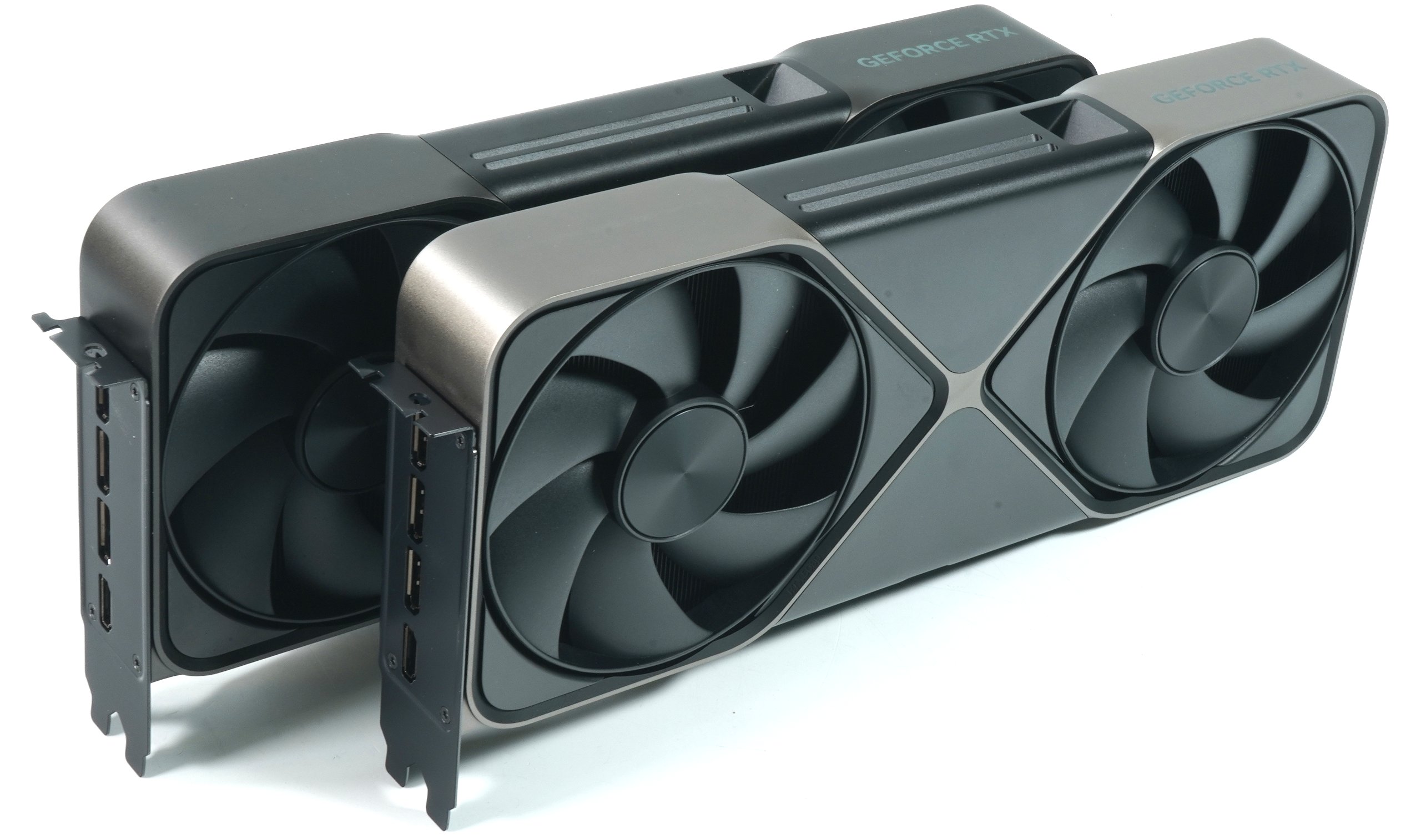
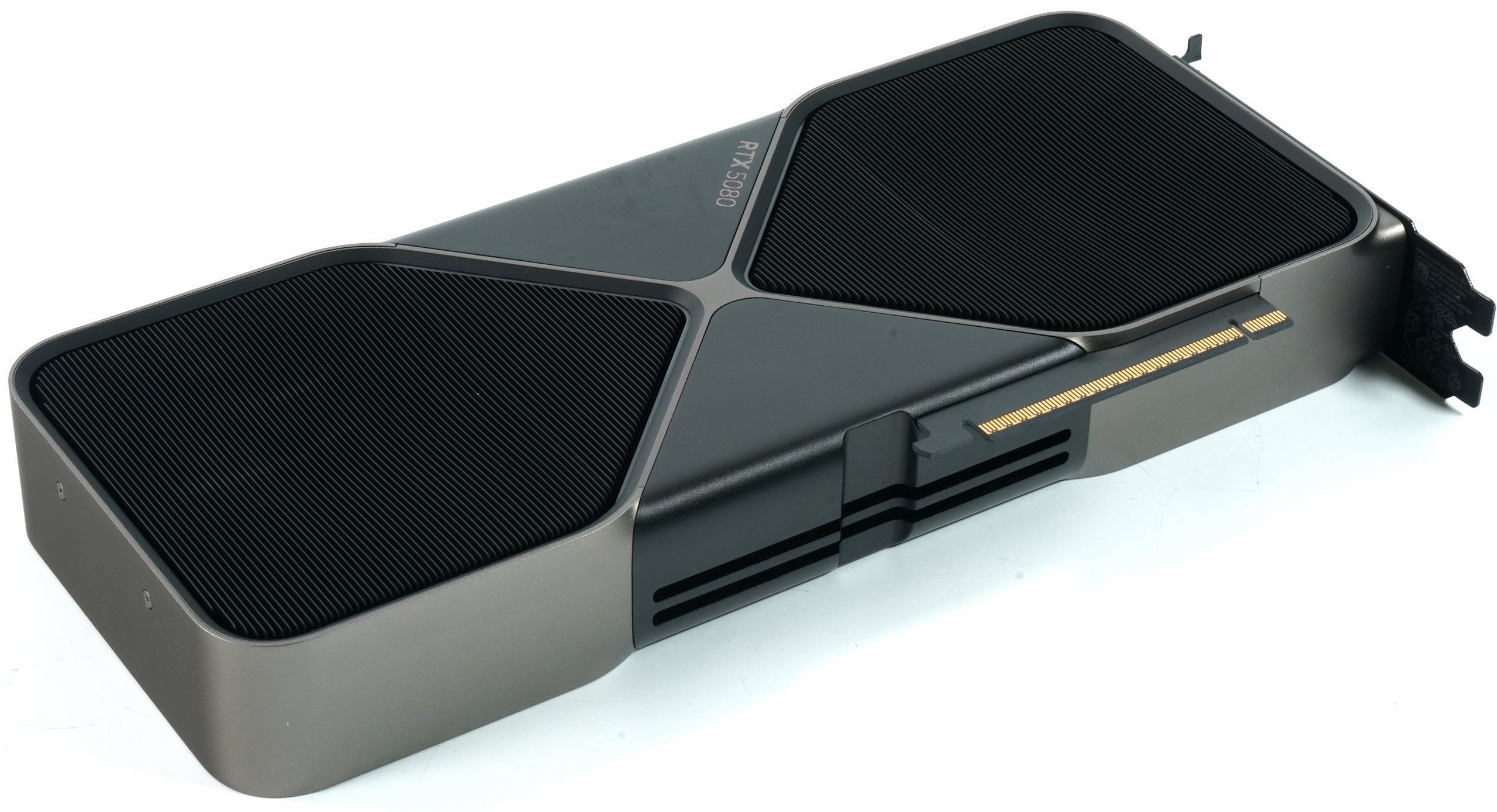
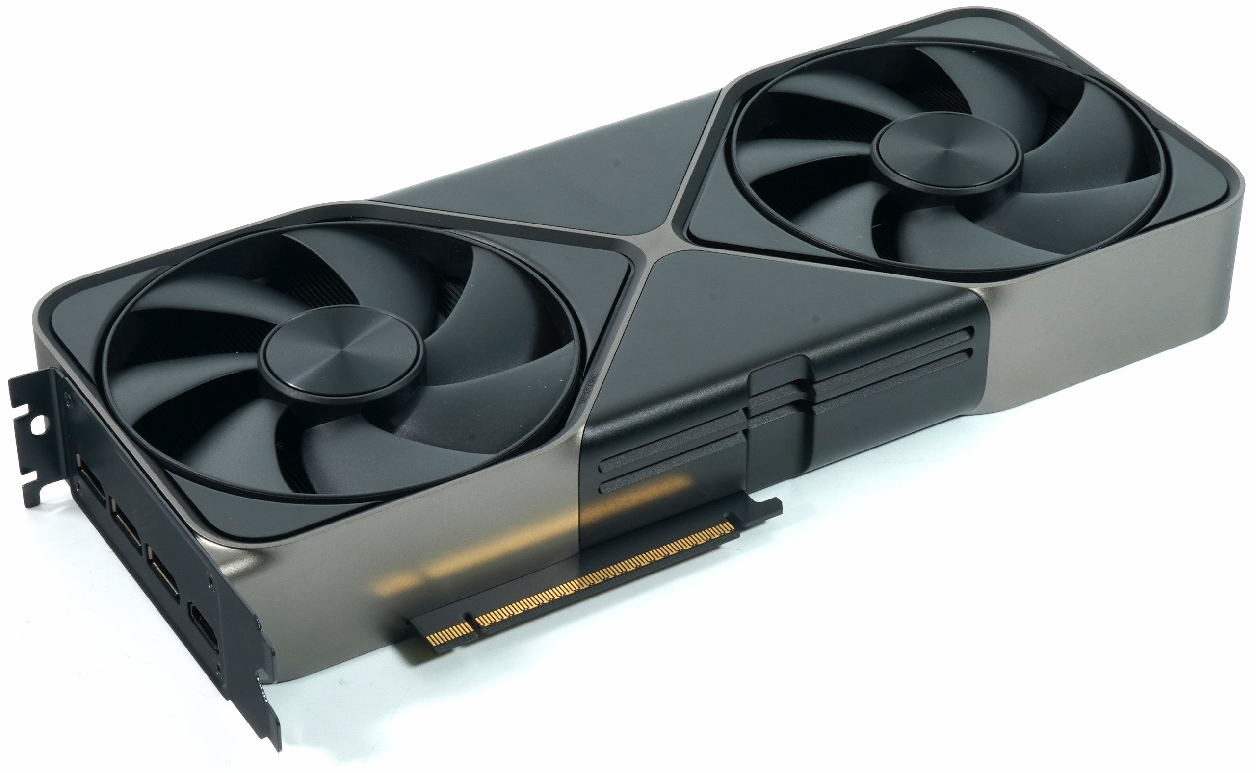
The card weighs just under 2 kilos and measures 304 mm in length, 137 mm in height and 48 mm in depth. An HDMI 2.1b port and three DisplayPort 2.1b interfaces are available for connecting external devices, while the card is integrated into the system via the PCIe 5.0 x16 interface.
The RTX 5080 supports DLSS 4 and offers decent performance for gaming in 4K at maximum graphics settings as well as for creative applications such as 3D rendering and video editing. The benchmarks will clarify the rest.
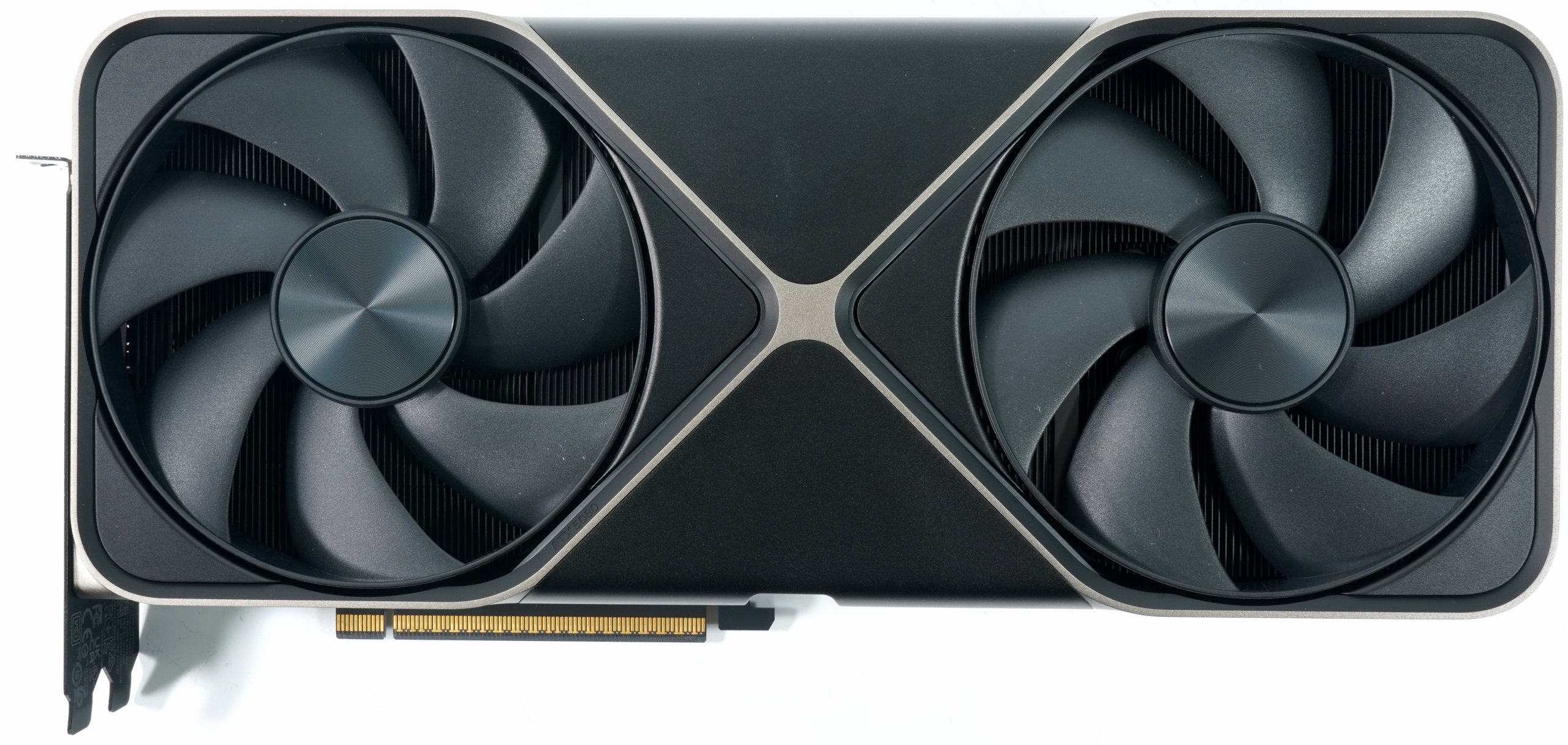
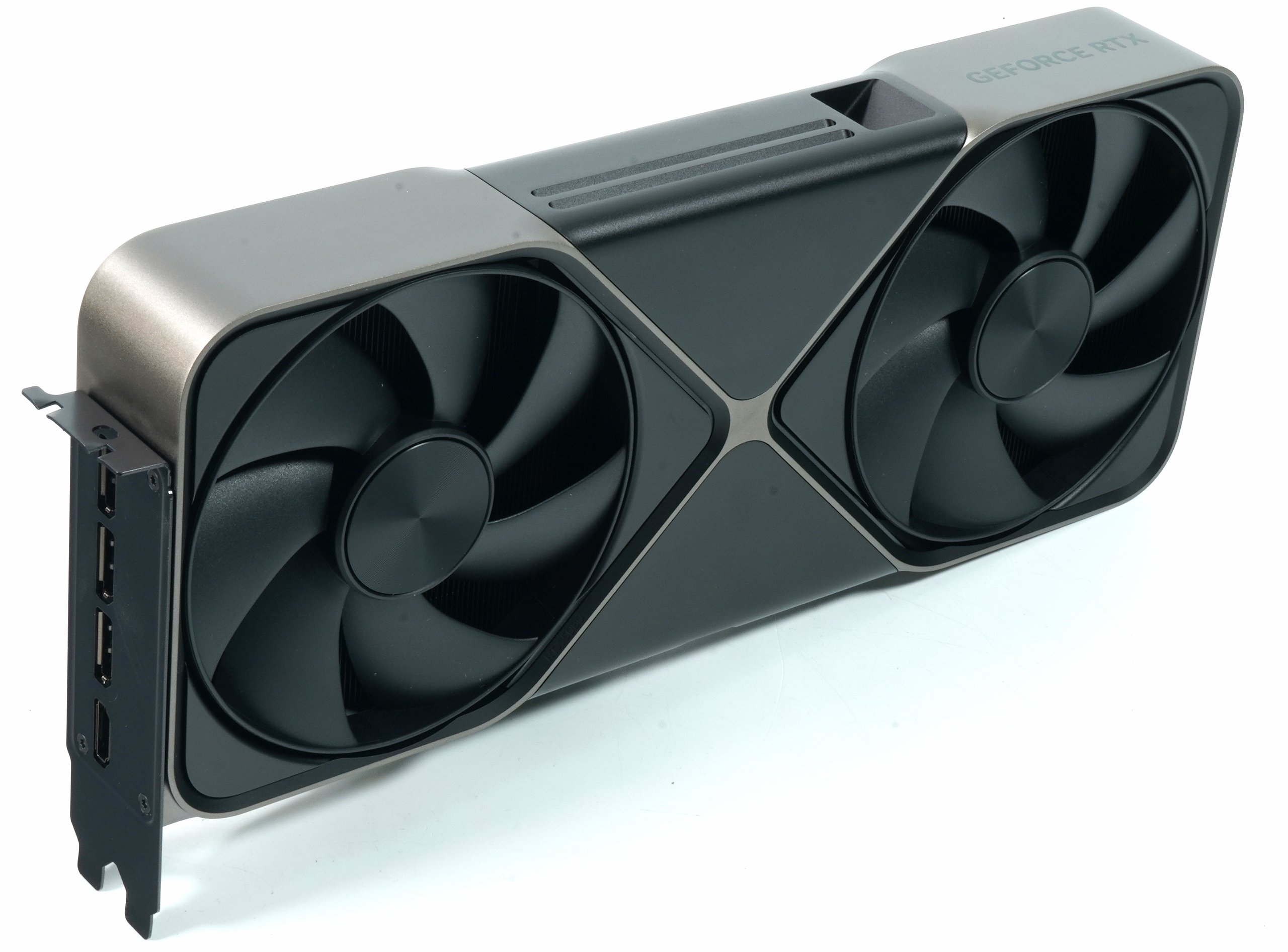
The GeForce RTX 5080 has a Thermal Design Power (TDP) of 360 watts (which can be increased to 390 watts) and is therefore positioned in a range that is unfortunately now typical for high-end graphics cards. This high power consumption is due to the fact that the card is based on the new Blackwell architecture and offers immense computing power, in particular thanks to 10,752 CUDA cores, 171 RT-TFLOPS and 56 shader TFLOPS. Despite the high TDP, the improved thermal design of the FE card, such as the double-flow cooling technology, ensures efficient heat dissipation and stable operation even under full load.
The table shows the remaining key data of the card tested today in comparison to its predecessors:
I’ll save myself any further architectural descriptions at this point and refer you to my launch article on the RTX 5090 FE and the MSI RTX 5090 SUPRIM SOC, for which I’ll then also explain the electrical details in more detail:
|
|

- 1 - Introduction and details of the Blackwell GB203-400-A1 GPU
- 2 - Test system and equipment
- 3 - Gaming: Full-HD 1920x1080 Pixels (Rasterization Only)
- 4 - Gaming: WQHD 2560x1440 Pixels (Rasterization Only)
- 5 - Gaming: Ultra-HD 3840x2160 Pixels (Rasterization Only)
- 6 - Gaming: WQHD 2560x1440 Pixels, Supersampling, RT & FG
- 7 - Gaming: Ultra-HD 3840x2160 Pixels, Supersampling, RT & FG
- 8 - DLSS4 and MFG: Cyberpunk 2077 in detail
- 9 - DLSS4 and MFG: Alan Wake 2 in detail
- 10 - PCIe Gen5 problems, power consumption and standards
- 11 - Load peaks and power supply recommendation
- 12 - Cooler, temperatures, thermography, noise development
- 13 - Summary and conclusion


181 Antworten
Kommentar
Lade neue Kommentare
Mitglied
Urgestein
Veteran
Urgestein
Veteran
Mitglied
Veteran
Veteran
Veteran
Veteran
Veteran
Urgestein
Mitglied
Veteran
Veteran
Urgestein
Urgestein
Urgestein
Urgestein
Alle Kommentare lesen unter igor´sLAB Community →